40,000 Square Feet of Cleanroom for the Post-Silicon Era: HCLTech Opens a ₹185 Crore Advanced Semiconductor Lab in Bengaluru
HCLTech launched a 40,000 sq ft Advanced Semiconductor Lab in Bengaluru with ₹185 crore of investment, betting that India's next chip opportunity is not fabs but the unglamorous engineering that happens after silicon comes back from the foundry.
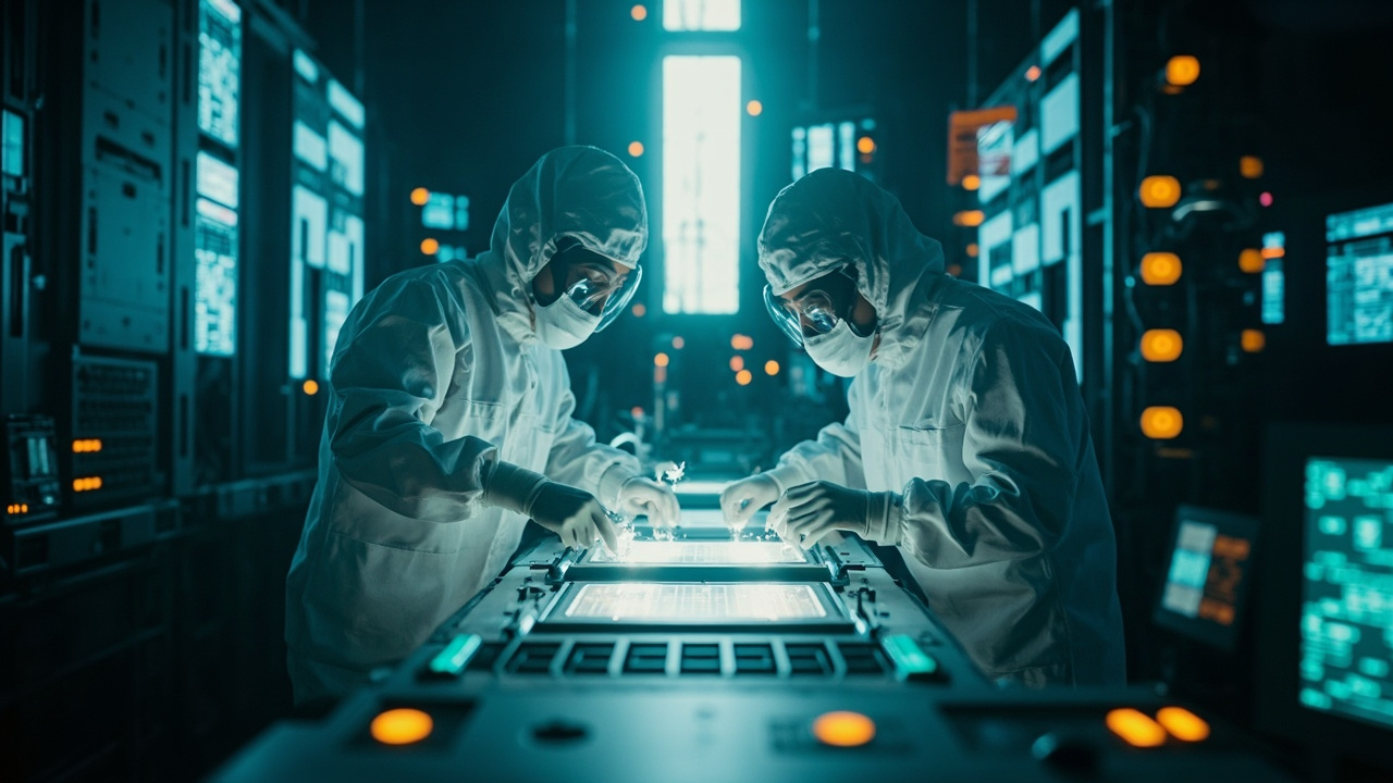
On Tuesday, September 8, 2026, HCLTech announced the launch of a state-of-the-art Advanced Semiconductor Lab in Bengaluru — a 40,000-square-foot facility built with an investment of ₹185 crore (roughly $22 million). The lab includes 25,000 square feet of Class 10K and Class 1K cleanrooms and is designed to deliver what the industry calls end-to-end post-silicon engineering: advanced testing, qualification, and failure analysis of chips after they come back from the fab.
At first glance, ₹185 crore is a rounding error next to the tens of billions flowing into AI datacenter buildouts this year. But the facility is a precise bet on where India’s semiconductor story actually makes money — and a signal that the country’s IT services giants intend to own the engineering layer of the chip economy, not just its code.
What the lab actually does
Post-silicon engineering is the discipline of validating and debugging manufactured silicon before it ships in products. When a foundry delivers a batch of prototype chips, someone has to bring them up, characterize their behavior across voltage, temperature and frequency corners, hunt down defects, and prove they meet reliability standards. It is meticulous, equipment-heavy work — and it has traditionally been concentrated in East Asia, the United States, and Israel.
The new Bengaluru lab is equipped for exactly this pipeline. According to HCLTech’s press release, the facility combines world-class cleanrooms with advanced testing, qualification, and failure-analysis capabilities in a unified environment. Reporting from the announcement indicates the test floor carries equipment from Teradyne, Advantest, and Keysight — the three names that dominate automated test and measurement worldwide.
The services portfolio spans several categories:
- Post-silicon validation and bring-up — characterizing new silicon against its design intent, exercising interfaces, and running corner tests before volume production.
- Advanced testing — automated test program development and execution on industrial-grade ATE platforms.
- Qualification and reliability — stress testing chips to automotive, industrial, and consumer reliability standards.
- Failure analysis — when a part misbehaves, physically localizing the defect and root-causing it, down to die-level inspection inside the cleanroom.
For fabless startups, hyperscalers building custom silicon, and global semiconductor companies, the pitch is a one-stop destination in India for everything that happens after tape-out.
Why this matters more than the price tag suggests
India’s semiconductor policy conversation is dominated by fabs — the India Semiconductor Mission has spent years and billions in incentives to attract fabrication plants and OSAT (assembly and test) facilities, with several projects now moving toward commercial production. But the quieter reality is that India’s strongest structural advantage in chips was never manufacturing scale. It is engineering talent: the country already supplies a large share of the world’s chip design workforce, embedded in the R&D centers of nearly every major semiconductor company.
HCLTech’s lab sits deliberately at the junction of those two stories. As physical fabs, ATMP lines, and OSAT plants come online in India, someone has to validate, test, and debug the silicon they produce — and the volumes of custom silicon being designed for AI workloads are exploding simultaneously. The lab lets HCLTech sell that capability as a service to global clients while the domestic ecosystem matures around it.
The market math is what turns a mid-sized capex line into a strategic move. Futurum Group’s analysis of the launch sizes the addressable channel opportunity at approximately $25.7 billion, and HCLTech’s semiconductor practice has been growing at a reported 19 percent CAGR. The lab is the physical infrastructure that lets an IT services firm capture high-value engineering work that pure software shops cannot touch — cleanrooms and ATE equipment are moats that take years and capital to replicate.
The services-firm playbook, rebuilt for silicon
There is a second layer to this announcement: it is a template for how India’s massive IT services industry is repositioning itself for the AI era. Traditional application development and maintenance contracts are under pressure from code-generating models; the growth frontier is shifting toward physical-digital hybrid engineering — chips, hardware validation, manufacturing systems, and the AI models that run on top of them.
HCLTech is not alone in reading the room. Rivals have been building out engineering R&D practices for years. What distinguishes this move is the willingness to put owned physical infrastructure — Class 1K cleanrooms, terabyte-scale test equipment — behind the services pitch. It converts HCLTech from a bodyshop-with-expertise into an infrastructure operator in the semiconductor value chain. The company will showcase the facility at SEMICON India 2026 in New Delhi later this month (September 17–19), alongside its “India Chip” OSAT collaboration, where the lab doubles as proof that India can serve the post-silicon needs of global clients today, not someday.
Context: the AI silicon boom is straining validation capacity
The timing is not accidental. The wave of custom AI accelerators — from hyperscaler in-house chips to the flood of inference silicon being designed for the agent economy — has created a validation bottleneck. Every new chip design needs post-silicon bring-up, characterization, and reliability qualification before it can ship, and the engineering capacity to do that work is scarce and geographically concentrated. Test-equipment makers have reported order books stretched by AI-related demand.
A 25,000-square-foot cleanroom in Bengaluru does not solve that problem globally. But it adds capacity exactly where the talent is cheapest relative to skill, and it gives AI chip designers a credible alternative to queueing behind hyperscaler priorities in East Asia or North America. In an industry where time-to-market for an accelerator can determine whether a startup survives, validation turnaround time is a real competitive variable.
What to watch
Three things will determine whether this is a milestone or a press release:
- Client traction. Whether global fabless companies and the new Indian fab/OSAT projects actually route validation work through the facility, rather than treating it as a showcase.
- Talent depth. Post-silicon engineering is a scarce skill even in India; the lab’s output depends on HCLTech training hundreds of engineers on ATE platforms and failure-analysis techniques.
- Ecosystem coupling. How tightly the lab integrates with the India Semiconductor Mission’s manufacturing projects and SEMICON-era partnerships like India Chip — services built around domestic fabs have a structural cost and logistics advantage.
For now, the signal is clear: the post-silicon layer of the chip economy is being contested, and India’s largest IT firms intend to compete for it with real infrastructure, not just resumes. A ₹185 crore cleanroom in Bengaluru is the opening move.
Sources
- [1] https://www.hcltech.com/en-us/press-releases/hcltech-launches-advanced-semiconductor-lab-rs-185-crore-investment
- [2] https://www.thehindu.com/business/hcltech-opens-advanced-semiconductor-lab-in-bengaluru/article71443763.ece
- [3] https://www.moneycontrol.com/news/business/information-technology/hcltech-invests-rs-185-crore-to-launch-advanced-semiconductor-lab-in-bengaluru-14025351.html/
- [4] https://www.techcircle.in/2026/09/08/hcltech-puts-185-cr-into-semiconductor-lab-as-chip-ecosystem-deepens
- [5] https://futurumgroup.com/insights/hcltechs-semiconductor-lab-bet-targets-a-257b-channel-opportunity/
- [6] https://www.aninews.in/news/business/hcltech-launches-rs-185-crore-semiconductor-testing-lab20260908150650