Samsung Puts Mistral AI Inside the Fab: On-Premises LLMs for Every Chip Plant
Announced during the Korea–France summit in Paris, Samsung's strategic partnership with Mistral AI brings Mistral Large and customized on-premises models into semiconductor design and manufacturing — defect detection, equipment optimization, and yield stabilization across memory, logic, and foundry.
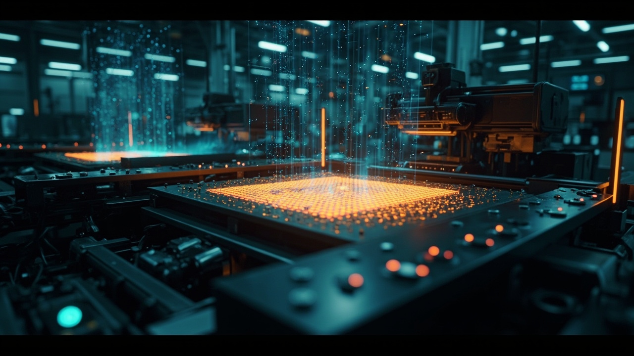
On the evening of September 8, in a press release timed to the state summit between South Korea and France in Paris, Samsung Electronics announced a strategic partnership with Mistral AI aimed squarely at the least glamorous and most consequential layer of the AI stack: the fab itself. Under the agreement, Samsung will integrate Mistral’s AI services and solutions — including its flagship large language model, Mistral Large — across its semiconductor operations, developing customized on-premises AI models optimized for what the two companies call “intelligence-driven infrastructure.”
The symbolism of the venue is hard to miss. The announcement was made during a state summit held in Paris between the two countries, casting a corporate technology deal as an act of industrial diplomacy between a Korean manufacturing giant and Europe’s highest-profile AI lab. Samsung has also led Mistral AI’s Series D funding round, securing a strategic equity stake to anchor the long-term collaboration — the operational sequel to Tuesday’s €3 billion raise, which valued the Parisian company at over €24 billion.
What Samsung is actually buying
Strip away the summit choreography and the deal has a precise technical shape. Samsung’s Device Solutions division — the unit that runs its memory, foundry, and system LSI businesses — will deploy Mistral’s AI platform inside its own semiconductor infrastructure. The engagement focuses on the development and implementation of on-premises AI technologies across Samsung’s chip operations, with Mistral Large serving as the foundation for customized models tuned to Samsung’s internal data and workflows.
The on-premises requirement is not a preference; it is the point. Semiconductor manufacturing generates some of the most sensitive industrial data in existence — process recipes, equipment telemetry, defect maps, yield statistics, all of it IP-adjacent and much of it export-control-relevant. The press release is explicit that the on-premises enterprise solutions “will especially ensure security and flexibility required to process highly sensitive technologies and operational data entirely within the boundaries of Samsung’s semiconductor infrastructure, maintaining total control over its mission-critical technologies.”
That is a sentence that could only be written by a company that has watched the last two years of cloud AI governance debates and concluded the answer for fabs is simple: the data never leaves. For Mistral, whose open-weight heritage and sovereign-AI positioning have made it the default European answer to “how do we get frontier-adjacent AI without handing our data to an American hyperscaler,” Samsung is the highest-value proof point yet that the strategy works for heavy industry, not just government clouds.
Where the models will work
The use cases named in the announcement are the classic bottlenecks of advanced chipmaking. As semiconductor processes become more advanced and complex, rapid data analysis in the fab is essential. By applying targeted AI models to defect detection and equipment optimization, Samsung aims to accelerate development cycles, manufacturing precision, and yield stabilization across its advanced memory and logic chips.
Defect detection is the canonical example. A modern leading-edge fab generates enormous volumes of inspection and metrology data; classifying, root-causing, and acting on anomalies faster directly translates into yield, and yield is the entire economics of memory manufacturing. Equipment optimization is the second pillar — predicting maintenance windows, tuning process chambers, and squeezing throughput out of machines that cost tens of millions of dollars each. LLM-driven systems add a layer beyond traditional statistical process control: ingesting engineering reports, logs, and documentation alongside sensor streams, and reasoning across them.
The framing “intelligence-driven infrastructure” suggests something broader than point solutions. Samsung’s own language — “a unique stack of tools that will transform how semiconductors are designed and manufactured” — points toward AI woven through the design-to-production pipeline, from EDA-adjacent design assistance to fab-floor decision support.
The quotes
“Increasing complexities involved in AI chip design and manufacturing requires continuous innovation in semiconductor technologies,” said Young Hyun Jun, Vice Chairman and CEO of the Device Solutions (DS) Division at Samsung Electronics. “We look forward to working with Mistral and supporting the evolving needs of customers, while delivering new breakthroughs across the semiconductor ecosystem essential to the AI era.”
“AI is reshaping how we build complex technologies, from silicon to software,” said Arthur Mensch, co-founder and CEO of Mistral. “We are proud to support Samsung Electronics with our expertise in electronics and semiconductors, helping to improve how chips are designed and manufactured, and to accelerate technical progress across the global semiconductor and AI value chain.”
Why this matters beyond the two companies
The deal lands in the middle of a structural shift in the AI industry: the biggest consumers of AI are increasingly the biggest manufacturers of AI hardware. Samsung is simultaneously the world’s largest memory maker, a foundry racing to close the gap with TSMC, and the supplier of HBM stacked memory that every AI accelerator on the planet depends on. If applying LLMs inside its fabs meaningfully improves yields or compresses development cycles at, say, its HBM4 or 2nm-class programs, the effect compounds across the entire AI supply chain — more usable HBM capacity, faster node transitions, and a stronger hand against SK Hynix in the memory race that underpins the GPU era.
For Mistral, the Samsung deal is the strongest validation yet of its pivot from consumer-of-attention chatbot to industrial and sovereign AI provider. The company spent 2026 signing compute partnerships (its multi-gigawatt Google and Broadcom TPU deal announced in April) and raising Europe’s largest-ever round; now it has an anchor customer that is also a shareholder. That alignment — Samsung leading the Series D and then deploying the technology in mission-critical operations — mirrors the capital-plus-customers pattern that defined the hyperscaler era, transplanted into European industrial AI.
There is also a competitive subtext. Samsung’s earlier collaboration with Dell on AI for fabs, its GTC-stage presence on agentic AI in manufacturing, and ASML’s own Mistral partnership (signed back in September 2025) sketch an industry converging on the same thesis: the next frontier of chipmaking efficiency is not a better lens or a bigger wafer, but models that can reason about the factory itself. Mistral now sits at the intersection of the two most strategically important equipment and manufacturing relationships in semiconductors.
What to watch
The partnership’s near-term deliverables will be invisible to consumers but legible to the industry: on-premises model deployments inside specific fabs, integration with Samsung’s existing fab automation stack, and eventually measurable outcomes in yield and cycle time that Samsung may choose to disclose at earnings. The strategic equity stake also raises the possibility of deeper co-development — Samsung silicon tuned for Mistral models, or Mistral models distilled for Samsung edge devices.
One open question is how the partnership interacts with Samsung’s consumer-facing AI ambitions, which remain anchored to Galaxy AI and partnerships elsewhere. The Mistral deal is deliberately narrow: it is about chips, not phones. That focus is a feature. The fab is where Samsung’s competitive position is most contested, and it is where AI applied well pays back fastest.
For an industry that has spent two years asking what AI can do for its own products, the Samsung–Mistral partnership is a reminder that the most durable returns may come from pointing AI at the production of the physical substrate everything else runs on. The fabs that learn fastest are about to have the advantage — and as of this week, one of the largest chipmakers on earth has decided its fab-tutor speaks French.
Sources
- [1] https://news.samsung.com/global/samsung-and-mistral-ai-announce-strategic-partnership-for-intelligence-driven-semiconductor-infrastructure
- [2] https://www.businesswire.com/news/home/20260908997770/en/
- [3] https://www.techbuzz.ai/articles/samsung-taps-mistral-ai-to-reboot-chipmaking-leads-funding
- [4] https://finance.yahoo.com/technology/ai/articles/samsung-mistral-ai-announce-strategic-161500934.html