Folding Silicon Instead of Shrinking It: Huawei's Kirin 9050 Pro Puts LogicFolding on Sale
Huawei's Kirin 9050 Pro is the first mass-market chip built on LogicFolding — stacking logic in vertical tiers to lift transistor density 55% without EUV lithography. It shipped inside the Mate XT 2 tri-fold this weekend.
On September 12, 2026, a phone went on sale in China that quietly marks one of the strangest turns in the semiconductor industry’s history. The Huawei Mate XT 2 Ultimate — a tri-folding handset with a 10.2-inch inner display and a starting price of RMB 19,999 (about $2,980) — is the first commercial product powered by a chip that abandons the industry’s core assumption: that progress means making transistors smaller.
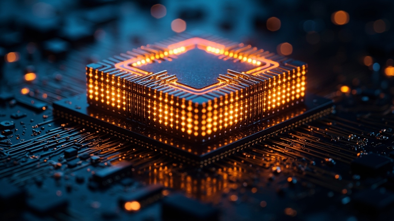
The Kirin 9050 Pro is the first mass-production silicon to use Huawei’s LogicFolding architecture, first unveiled publicly in May 2026 at the IEEE ISCAS symposium alongside the company’s “τ (tau) scaling law.” Instead of etching ever-finer features with extreme ultraviolet (EUV) lithography — equipment Huawei cannot legally buy because of US export controls — the design folds logic circuits into vertically stacked tiers, bridged by dense arrays of vertical interconnects. Signals travel shorter distances; the chip gets faster and more efficient without a single new manufacturing node.
The Numbers Huawei Claims
According to specifications released at the September 7 launch event and reported by TechNode, the Kirin 9050 Pro lifts transistor density from 155 MTr/mm² to 238 MTr/mm² — a 53.5% jump — without touching conventional geometric scaling. Performance cores reach 3.1 GHz peak frequency. The area consumed by the chip’s high-speed global on-chip network is cut by 55%, and SRAM operating frequency rises by more than 40%.
The CPU side uses Huawei’s Lingxi hyperthreading technology: peak single-core performance is up 24% over the previous generation, multi-core up 52%. On the graphics side, the Maleoon GPU adds hardware-accelerated real-time ray tracing with up to 50 million calculations per frame cycle. The Da Vinci NPU architecture is optimized for multi-sized on-device large models — a direct answer to the industry’s push for local AI inference.
At the system level, Huawei claims the chip-plus-HarmonyOS 7 combination extends battery life by an additional 36 minutes, and overall device performance in the Mate XT 2 is 42% higher than the previous-generation Mate XT.
Why Heat Was Supposed to Kill This Idea
When Huawei presented LogicFolding at ISCAS in May, the sharpest objection from the audience was thermal. Stack active transistors on top of active transors, pack more of them into every square millimeter, and seal the result inside a compact mobile device — the physics seems inevitable: power becomes heat, trapped heat throttles clocks and eventually cooks the chip.
A September 3 paper on arXiv (arXiv:2609.04287), authored by Huawei’s Tingbo He — the same executive who presented the τ scaling law at ISCAS — claims measurements on real silicon show the opposite. The Kirin 2026 silicon is cooler than its predecessor while packing 55% more transistors per square millimeter and delivering as much as 66% power reduction on some key workloads.
The explanation is one Huawei frames in an unusually literary register for a chip paper: “on a chip, as in a workday, it is the travel that burns the majority of the energy, not the work at the desk.” In modern SoCs, a large share of dynamic power is spent driving signals across long horizontal interconnects. By folding circuits into tiers connected by vertical links — built with 3D hybrid bonding, a process closer to welding than packaging — the wires get dramatically shorter, and the RC (resistance-capacitance) tax on every signal falls with them.
The enabling craft is 3D hybrid bonding: two wafers aligned, pressed together, and slowly heated until covalent bonds form across the oxide surfaces and copper pads fuse into continuous metal. Where today’s most advanced commercial logic chips place vertical connections about 10 μm apart — fewer than 1 million links per 100 mm² — LogicFolding needs bonding pitch in the 1.5–1 μm range to genuinely cut RC. That is the real manufacturing frontier here, not lithography.
The Sanctions Angle: Scaling Time Instead of Space
The strategic backdrop is impossible to ignore. Shrinking past the 7-nanometer node requires EUV lithography, and ASML’s EUV machines cannot be sold to China under US export controls. Huawei’s answer, developed over roughly six years, is to reappraise geometric scaling for what it always was — a means, not an end. The point of smaller transistors was never smallness itself, but the things smallness delivered: faster switching, shorter response times, higher clocks.
τ scaling law is the formalization: a campaign to drive down the characteristic delay (τ) a signal takes across a chip’s critical paths, generation after generation. LogicFolding is its flagship technique at the circuit and chip levels; the framework extends to devices and whole systems. Huawei has said it targets 1.4nm-equivalent density by 2031 on this roadmap.
Skeptics note that “LogicFolding” is, at bottom, an aggressive application of 3D stacking and hybrid bonding — technologies the wider industry is also pursuing, just less urgently because it can still buy EUV. The Reddit thread on the original announcement put it bluntly: it’s hybrid bonding and chip stacking with a marketing name. That critique is fair as far as it goes, but it undersells the engineering reality: doing this at flagship-phone volumes, yields, and thermal envelopes is a genuinely hard problem that no other company has attempted in consumer silicon, precisely because everyone else has an easier path.
Why a Tri-Fold Phone Is the Testbed
The Mate XT 2 Ultimate is an unusual vessel for a chip breakthrough — a $2,980 luxury tri-fold with a 6.5-inch outer display, 10.2-inch inner display, 299-gram chassis, 5,600 mAh battery, and 50W wireless charging. But the choice is strategic. As TechNode notes, the chip-plus-HarmonyOS 7 integration matters more for a tri-fold than a conventional slab: the larger display and more complex form factor place greater demands on performance scheduling, power efficiency, multitasking, and app compatibility. The device is a demonstration that Huawei’s stack — chip, OS, and hardware co-designed — can keep a exotic form factor competitive.
The Kirin 9050 Pro is also the first new Kirin chip introduced at a flagship launch in six years, a symbolically loaded milestone for a company written off by many after 2019’s sanctions.
What to Watch
The honest caveat is that Huawei’s numbers are Huawei’s numbers. Independent benchmarks of the Mate XT 2 will tell us whether the 42% performance uplift and thermal claims hold in shipping hardware, and teardowns will reveal the real manufacturing story behind the 238 MTr/mm² density figure. The arXiv paper’s power measurements, while detailed, come from the company that sells the chip.
But the direction is clear, and it is bigger than one phone. If architectural scaling — folding, stacking, shortening — can substitute for even part of what EUV lithography buys, then the semiconductor industry’s map splits in two: a Western roadmap that keeps paying more for each new node, and a Chinese roadmap that scales time instead of space. The Kirin 9050 Pro going on sale September 12 is the first consumer-visible data point in that divergence. For an industry that has spent fifty years assuming there is only one road forward, that alone makes it one of the most consequential chip launches of the year.
Sources
- [1] https://technode.com/2026/09/08/huawei-unveils-kirin-9050-pro-chip-debuts-new-mate-xt-2-tri-folding-smartphone/
- [2] https://arxiv.org/html/2609.04287v1
- [3] https://www.huawei.com/en/news/2026/5/ieee-iscas-tau-scaling
- [4] https://www.lightreading.com/smartphones-devices/huawei-puts-pioneering-chip-design-tech-to-its-first-test
- [5] https://www.scmp.com/tech/big-tech/article/3366669/huaweis-new-kirin-chip-puts-logicfolding-test-bigger-ambitions