The Chip That Wrote Itself: openTPU Runs Qwen3 on an FPGA Its Agents Designed
A single GitHub committer claims AI agents designed a full-stack inference accelerator — RTL, ISA, compiler and all — and it now runs ten open models bit-exactly on a $200 Kintex-7 FPGA card.
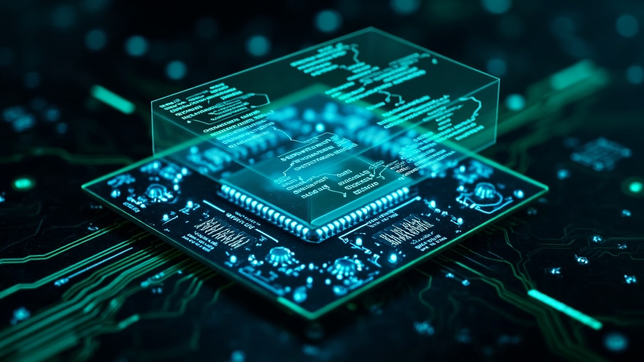
Sometime in late September, a GitHub user named FeSens pushed a repository with a tagline that reads like a riddle: “An open-source AI accelerator, developed by AI.” By October 6–7, the project — openTPU — had hit Hacker News and the AI press, and the riddle had a punchline: a complete inference accelerator stack, from SystemVerilog RTL up through a custom instruction set, a kernel language and compiler, a bit-exact simulator, a profiler, and host tooling that drives a real PCIe FPGA card. All of it, the author says, was built with heavy help from AI agents. And the card works: it runs ten open-weight language models with their real weights, producing tokens that match the simulator bit for bit.
What’s actually in the repo
openTPU is a full monorepo, and that is the point. The stack reads bottom-up like a computer-architecture textbook with working code at every layer:
- Hardware (SystemVerilog RTL) targeting a Xilinx Kintex-7 xc7k480t FPGA on an Inspur YPCB-00338 PCIe card, with 4 GiB of DDR3-1066 across two channels and a 17.1 GB/s memory peak. The production image runs at 133.33 MHz.
- A custom ISA where every instruction is 8×32-bit words, and an ISA simulator in Python that is checked against the RTL bit-for-bit by the test suite.
- A kernel language (“ol”) and compiler with layouts, affine loop addressing, and fusion — you write
@ol.jit-decorated Python kernels for MLP, attention, and full model layers. - Lens, a profiler that records a run from the RTL, simulator, or the physical card and replays it in a browser with a roofline, a timeline, and per-instruction tables.
- Host tools:
otpu-chatfor chatting with the models,otpu-smifor temperature, power, DRAM bandwidth and per-unit utilization, plus selftest and diagnostics.
The machine is deliberately simple and completely legible. A sequencer issues one instruction per cycle to a handful of units: DMA moves data, a four-column systolic matrix unit multiplies int8 weights streamed from DRAM, a vector unit does fp32 math, and a quantizer rounds results back to int8. “There is no cache and no hidden scheduling: every data movement is an instruction, so a trace shows exactly where the cycles go.”
The numbers
The results table is where the project stops being a thought experiment. On the physical card, measured across late September and October 1:
| Model | Weights | Decode | DRAM use |
|---|---|---|---|
| LFM2.5-230M | int8 | 59.0 tok/s | 85% of peak |
| LFM2.5-230M | 4-bit + int8 head | 85.8 tok/s | 82% |
| Qwen3-0.6B | int8 | 21.6 tok/s | 84% |
| Qwen3.5-0.8B | 4-bit | 24.5 tok/s | 83% |
| SmolLM3-3B | 4-bit | 8.74 tok/s | 92% |
| Qwen3.5-4B | 4-bit | 5.88 tok/s | 92% |
Decode runs at 82–94% of the card’s DRAM peak — the telltale signature of a memory-bound design, which is exactly what you want a small-batch inference engine to be. Prefill reaches 295.6 tok/s on the 230M model. The 4-bit path uses FP4 values with two-level block scales (4.25 bits per weight) and keeps the LM head in int8, cutting bytes per token by roughly a third and lifting decode 40–45%.
Two mixture-of-experts models larger than the card’s memory run with experts streamed from host storage: LFM2.5-8B-A1B hits 10.6 tok/s with 98.5% of expert uses found in on-card slots, and Qwen3.5-35B-A3B manages 3.95 tok/s with 153 MB streamed per token over PCIe. Both, the README says, match the simulator bit for bit.
How the “developed by AI” part worked
The provenance is the project’s boldest claim. openTPU descends from FeSens’s earlier auto-arch-tournament, and the method is an automated hill climb: each round, several LLM agents read one hardware component and propose a change; another agent writes it. A candidate only survives if it passes lint checks, bit-exact tests against the simulator, a cycle-count check, and performance tests — and it is kept only if it is smaller at the same speed, or faster at the same size. The first overnight run tried 96 changes across six components and kept 38. The estimated clock for the accelerator logic went from 41 MHz to 106 MHz, and area from 132K down to 82K lookup tables.
The caveats are real, and the deeper reporting (notably TrackFuture’s analysis) does not hide them: those are yosys estimates rather than Vivado results, they exclude the PCIe and DDR3 controllers, and “manual fixes” were involved — one Hacker News commenter described the setup fairly as “an experienced person pointing an LLM in a tasteful direction.” The README also does not quantify the agent-versus-human split, or name the harness and models used. And the tagline’s second question — can agents build the chip that runs their own inference — is rhetorical: the card runs 0.2–4B open models, not the agents that wrote the design.
Why it matters anyway
Strip away the hype and two things remain genuinely significant.
First, verification as the engine of automation. The tournament worked because the gate was merciless: every change had to match a simulator bit for bit before it counted. That is the same lesson as formal-proof systems — AI output becomes useful when something other than the AI can check it. Chip design, where a wrong wire costs a tape-out, is precisely the domain where this pattern generalizes. It is the pattern behind OpenAI’s internally-designed Jalapeño chip too, reported last month: models pointed at design and benchmark software with strong checks underneath.
Second, the cost floor for exploratory accelerator design just dropped. As AI Weekly’s editor put it, a single-committer stack claiming agents designed its RTL, ISA, and compiler is “cheap to dismiss and hard to replicate; if the methodology holds up, the cost floor for exploratory in-house accelerator design drops, and ‘read the whole monorepo’ becomes an on-ramp to accelerator literacy that neither Nvidia nor Google can match on openness.” For students and small teams, everything except the card runs on a laptop: pip install -e ., pytest, Verilator 5 for the RTL tests, then otpu-chat --backend isa to chat with Qwen3-0.6M on the simulator.
An FPGA can be reprogrammed to test a new design; custom silicon cannot be changed once made. Whether agent-driven design survives contact with real fabrication costs and verification at scale is a prediction, not a finding. But as a proof of concept — and as the most readable end-to-end accelerator codebase in the open — openTPU is worth your evening.
Sources
- [1] https://github.com/FeSens/openTPU
- [2] https://aiweekly.co/alerts/github-opentpu-ships-ai-designed-fpga-inference-accelerator-running-qwen3-and
- [3] https://news.ycombinator.com/item?id=49980715
- [4] https://trackfuture.ai/article/can-ai-agents-design-the-chip-they-run-on-inside-opentpu
- [5] https://aicoder.com/news/news-20261007-opentpu-ai-designed-open-source-accelerator-fpga